CIA
Description[edit | edit source]
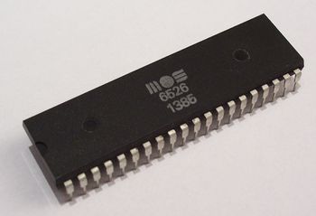
The CIA (Complex Interface Adapter) is an interface chip used in the Commodore homecomputer. It controls most of the I/O processes and contains as well the internal timer (clock). The CIA was developed from the Semiconductor manufacturer MOS Technology, which was taken over in 1976 by Commodore. Inside the C64 there are two CIA 6526 chips used; later C64-versions may also use the 6526A or the 8521.
Details of the CIA 6526[edit | edit source]
- 16 single programmable In- and Output lines
- The lines are lead through open collector with internal pullups.
- In the C64 some of these lines are used to monitor/control the I/O devices (keyboard, joystick, iec, etc.), some are connected with the VIC to define which area of memory it can address, others are for free disposition and are available at the userport.
- 8- or 16-Bit data transport (reading or writing) with handshaking.
- 2 independent 16-bit interval timers
- each timer consists of a 16 bit-latch (start value) and the actual 16 bit-timer
- the latch can be set directly, the timer can only be read indirectly via the latch.
- 24-h-timeclock (AM/PM) with programmable alarm
- 8-bit shift register for serial In- and Output.
- 2 TTL-inputs
- CMOS-compatible
- Pulsing: 1 MHz (6526) or 2 MHz (6526A)
Memory addresses of the CIAs[edit | edit source]
The following memory addresses are used from the two CIA-Chips in the C64:
CIA 1[edit | edit source]
Paddles,| Address area: $DC00-$DCFF, 56320-56575 Tasks: Keyboard, Joystick, Paddles, Datasette, IRQ control | ||||
| Address Hex |
Address Dec |
Register | Function | Remark |
|---|---|---|---|---|
| $DC00 | 56320 | 0 PRA |
Data Port A | Monitoring/control of the 8 data lines of Port A. The lines are used for multiple purposes: Read/Write: Bit 0..7 keyboard matrix columns |
| $DC01 | 56321 | 1 PRB |
Data Port B | Monitoring/control of the 8 data lines of Port B. The lines are used for multiple purposes: Read/Write: Bit 0..7 keyboard matrix rows |
| $DC02 | 56322 | 2 DDRA |
Data Direction Port A |
Bit X: 0=Input (read only), 1=Output (read and write) |
| $DC03 | 56323 | 3 DDRB |
Data Direction Port B |
Bit X: 0=Input (read only), 1=Output (read and write) |
| $DC04 | 56324 | 4 TA LO |
Timer A Low Byte |
Read: actual value Timer A (Low Byte) Writing: Set latch of Timer A (Low Byte) |
| $DC05 | 56325 | 5 TA HI |
Timer A High Byte |
Read: actual value Timer A (High Byte) Writing: Set latch of timer A (High Byte) - if the timer is stopped, the high-byte will automatically be re-set as well |
| $DC06 | 56326 | 6 TB LO |
Timer B Low Byte |
Read: actual value Timer B (Low Byte) Writing: Set latch of Timer B (Low Byte) |
| $DC07 | 56327 | 7 TB HI |
Timer B High Byte |
Read: actual value Timer B (High Byte) Writing: Set latch of timer B (High Byte) - if the timer is stopped, the high-byte will automatically be re-set as well |
| $DC08 | 56328 | 8 TOD 10THS |
Real Time Clock 1/10s |
Read: Bit 0..3: Tenth seconds in BCD-format ($0-$9) |
| $DC09 | 56329 | 9 TOD SEC |
Real Time Clock Seconds |
Bit 0..3: Single seconds in BCD-format ($0-$9) Bit 4..6: Ten seconds in BCD-format ($0-$5) |
| $DC0A | 56330 | 10 TOD MIN |
Real Time Clock Minutes |
Bit 0..3: Single minutes in BCD-format( $0-$9) Bit 4..6: Ten minutes in BCD-format ($0-$5) |
| $DC0B | 56331 | 11 TOD HR |
Real Time Clock Hours |
Bit 0..3: Single hours in BCD-format ($0-$9) Bit 4..6: Ten hours in BCD-format ($0-$5) |
| $DC0C | 56332 | 12 SDR |
Serial shift register |
The byte within this register will be shifted bitwise to or from the SP-pin with every positive slope at the CNT-pin. |
| $DC0D | 56333 | 13 ICR |
Interrupt Control and status |
CIA1 is connected to the IRQ-Line. Read: (Bit0..4 = INT DATA, Origin of the interrupt) |
| $DC0E | 56334 | 14 CRA |
Control Timer A | Bit 0: 0 = Stop timer; 1 = Start timer Bit 1: 1 = Indicates a timer underflow at port B in bit 6. |
| $DC0F | 56335 | 15 CRB |
Control Timer B | Bit 0: 0 = Stop timer; 1 = Start timer Bit 1: 1 = Indicates a timer underflow at port B in bit 7.
Bit 7: 0 = Writing into the TOD register sets the clock time, 1 = Writing into the TOD register sets the alarm time. |
| $DC10-$DCFF | 56336-56575 | - | - | The CIA 1 register are mirrored each 16 Bytes |
CIA 2[edit | edit source]
The second CIA-chip is identical to the first. Therefore in the following table are only entries which are specific to the usage in the C64.
| Address range: $DD00-$DDFF, 56576-56831 Tasks: Serial bus, RS-232, VIC memory, NMI control | ||||
| Address Hex |
Address Dec |
Register | Function | Remark |
|---|---|---|---|---|
| $DD00 | 56576 | 0 PRA |
Data Port A | Bit 0..1: Select the position of the VIC-memory
Bit 2: RS-232: TXD Output, userport: Data PA 2 (pin M)
Bit 6..7: serial bus Input (0=Low/Active, 1=High/Inactive)
|
| $DD01 | 56577 | 1 PRB |
Data Port B | Bit 0..7: userport Data PB 0-7 (Pins C,D,E,F,H,J,K,L) The KERNAL offers several RS232-Routines, which use the pins as followed:
Bit 1..5: RS-232: writing
|
| $DD02 | 56578 | 2 DDRA |
Data direction Port A |
see CIA 1 |
| $DD03 | 56579 | 3 DDRB |
Data direction Port B |
see CIA 1 |
| $DD04 | 56580 | 4 TA LO |
Timer A Low Byte |
see CIA 1 |
| $DD05 | 56581 | 5 TA HI |
Timer A High Byte |
see CIA 1 |
| $DD06 | 56582 | 6 TB LO |
Timer B Low Byte |
see CIA 1 |
| $DD07 | 56583 | 7 TB HI |
Timer B High Byte |
see CIA 1 |
| $DD08 | 56584 | 8 TOD 10THS |
Real Time Clock 1/10s |
see CIA 1 |
| $DD09 | 56585 | 9 TOD SEC |
Real Time Clock Seconds |
see CIA 1 |
| $DD0A | 56586 | 10 TOD MIN |
Real Time Clock Minutes |
see CIA 1 |
| $DD0B | 56587 | 11 TOD HR |
Real Time Clock Hours |
see CIA 1 |
| $DD0C | 56588 | 12 SDR |
Serial shift register |
see CIA 1 |
| $DD0D | 56589 | 13 ICR |
Interrupt control and status |
CIA2 is connected to the NMI-Line. Bit 4: 1 = NMI Signal occured at FLAG-pin (RS-232 data received) |
| $DD0E | 56590 | 14 CRA |
Control Timer A | see CIA 1 |
| $DD0F | 56591 | 15 CRB |
Control Timer B | see CIA 1 |
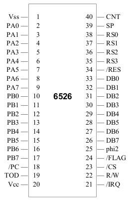
Pinout[edit | edit source]
Failure Symptoms[edit | edit source]
CIA 1
- Startup screen normal, but no cursor.
- No keyboard or control port access but cartridge works.
- Partial failure: some keys or joystick positions don't work, one character appears ahead of startup cursor or random characters appear at startup. Blank screen if chip is shorted (remove to check) and chip may get hot to the touch.
CIA 2
- Startup screen normal.
- No serial or user port access.
- "File not found" error when drive accessed.
- Cartridge works.
- Characters may show as blocks on startup screen.
Links[edit | edit source]
| Wikipedia: MOS_Technology_CIA |
- MOS 6526 CIA data sheet (PDF Format)
- Mapping the C64 - e.g. details about programming the CIA
- The CIA 6526 in the Commodore Computer Online Museum

Hardware internals of the C64 · Hardware portal
Components of the C64: CPU · VIC · SID · CIA · PLA · RAM · ROM · Color RAM

